tagbase-v7
The original tag base, and the one most of the project's current measurements were made on. A finished tag sits in a 3D-printed holder and six spring-loaded pogo pins press on the test pads on its underside.
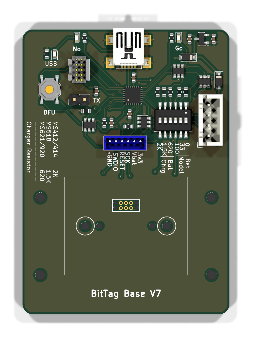
Block diagram
flowchart TB
  subgraph IF["External interface"]
    direction LR
    MCU["STM32F042G6<br/>ST-LINK emulation"]
    REG["XC6206 regulator"]
    USB["USB Mini-B (J104)"]
    SWD["SWD header (J102)"]
  end
  subgraph PWR["Power and measurement"]
    direction LR
    CHG["4 × 620 Ω charge array<br/>+ 4-way DIP switch"]
    MODEL["33 Ω / 100 Ω<br/>battery models"]
    SW["4 × TS5A3159<br/>analog switches"]
    EXT["EXT_PWR (J1)<br/>Joulescope"]
  end
  subgraph TGT["Target interface"]
    POGO["6-pin pogo connector (J101)<br/>6pin_tagpoints_new_offset"]
  end
  IF --- PWR
  PWR --- TGT
Major components
| Role | Part | Notes |
|---|---|---|
| Programming processor | STM32F042G6 | Emulates ST-LINK so openocd and st-util work unmodified |
| Regulator | XC6206 | |
| Supply switching | TS5A3159ADBVR ×4 | Low-leakage analog switches on TAG_3V3_EN, TAG_VBAT_EN and ADC_EN |
| Charger | 4 × 620 Ω + SW_DIP_x04 |
A coin cell charges from 3.3 V through a resistor; the switch picks which |
| Battery models | 33 Ω, 100 Ω | Sized to the internal resistance of real cells |
| Target connector | 6pin_tagpoints_new_offset |
Pogo pins onto the tag's six test pads |
| Indicators | Red and green LEDs, tactile switch |
What is distinctive
Four independently gated supply paths. This is the most elaborate of the
four bases in how it controls power to the tag, and the only one where the
gating is electronic rather than mechanical throughout. TAG_3V3_EN,
TAG_VBAT_EN and ADC_EN are firmware-controlled, so a measurement sequence
can be scripted rather than set by hand.
An analog switch works here because the coin cell it serves is not a cell: it is 3.3 V through a selected resistor of several hundred ohms, against which the switch's own on-resistance and leakage barely register. The LiPo bases cannot make that trade and use a physical changeover instead — see the overview.
Three directories, and which one this is
Three copies of this board live in the repository, and until 2026-10-08 the
documentation described the wrong one. They are told apart by R6, not by
the silkscreen: both 2023 copies are marked BitTag Base V7 and dated
5/31/2023 on the board itself.
| Directory | R6 |
Fabricated |
|---|---|---|
Bases/tagbase-v7 — this board |
100 Ω | yes, production/gerber.zip |
Obsolete/tagbase-jlcpcb-v7 |
82 Ω | no |
Obsolete/tagbase-jlcpcb-v3 |
— | the 2020 V3b |
The two 2023 layouts place all forty parts identically, so only R6 and
the silkscreen legend distinguish them. The oldest board's own title block
reads "V3b (marked V7)", which is why a V7 marking proves nothing.
Earlier notes and the tagbase-lipo-v1 design review call this board
tagbase-jlcpcb-v7. That name now belongs to the 82 Ω revision that was
never built.
Design files
Design directory on GitHub Schematic (PDF)
No design review has been written for this board.