tag-breakout-l432v2
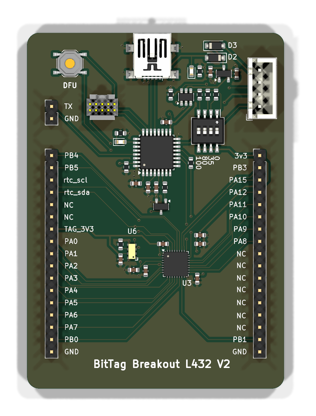
A breakout base for the STM32L432 tag line. It carries the half of a tag that is not being prototyped — processor and real-time clock — and exposes the rest on a pair of 1×17 headers for a prototype board to plug into.
Known wiring error: the RTC's SDA and SCL are swapped
On this board the two I²C lines between the processor and the RV-3028 are crossed at the processor:
| STM32L432KC pin | Alternate function (AF4) | Wired to |
|---|---|---|
29 — PB6 |
I2C1_SCL |
RTC SDA (U6 pin 4) |
30 — PB7 |
I2C1_SDA |
RTC SCL (U6 pin 3) |
The RTC end and the 1×17 header (J3 pins 3 and 4) are consistent with each
other, so the crossing is specifically between the processor and the rest of
the bus. tag-breakout-l432v1 was wired the right way round; the swap was
introduced in v2.
Nothing reports this. Peripheral I²C1 drives the wrong wires, the bus never
acknowledges, and the symptom looks like a dead or unpopulated RTC. It is a
defect in this board, not in the firmware under test, and it does not affect
the tags themselves or the
u375 breakout base, which wires PB6 to
rtc_scl and PB7 to rtc_sda as the datasheet intends.
The workaround is to drive the clock in software (bit-banged on the swapped pins) or to bodge the two nets.
Block diagram
flowchart TB
  subgraph IF["External interface"]
    direction LR
    MCU["STM32F042K6<br/>ST-LINK emulation"]
    REG["XC6206 regulator"]
    USB["USB Mini-B (J104)"]
    SWD["SWD header (J102)"]
  end
  subgraph PWR["Power and measurement"]
    direction LR
    CHG["Charge resistor array<br/>+ 4-way DIP switch"]
    SW["TS5A3159<br/>analog switch"]
    EXT["EXT_PWR / PWR_IN (J1)<br/>Joulescope"]
  end
  subgraph TAG["Tag side — what a tag would carry"]
    direction LR
    TMCU["STM32L432<br/>tag processor"]
    RTC["RV-3028-C7<br/>RTC"]
  end
  subgraph CONN["Prototype interface"]
    PAIR["J3 + J4<br/>2 × 1×17 header"]
  end
  IF --- PWR
  PWR --- TAG
  TAG --- CONN
Major components
| Role | Part | Section |
|---|---|---|
| Programming processor | STM32F042K6 | External interface |
| Regulator | XC6206 | External interface |
| Supply switching | TS5A3159ADBVR | Power — coin-cell line, so a low-leakage analog switch |
| Charge selection | SW_DIP_x04 with 620 Ω resistors |
Power |
| Tag processor | STM32L432 | Tag side |
| Tag RTC | RV-3028-C7 | Tag side |
| Reset | Q_NPN_BEC + Schottky ×2 | Tag side |
| Prototype interface | J3, J4 — PinHeader_1x17 |
Connector pair |
What is distinctive
No regulator on the tag side. The STM32L432 runs directly from the supply, as it does on the tag boards themselves. The U375 breakout needs one; this does not.
It prototypes the L432 tags. Pair it with UIUCBreakout, whose ADXL367, BMP585 and AT25FF321A are exactly the sensor set of the UIUC tag.