tag-breakout-u375-smps-v1
The breakout base for the STM32U375 tag line — the line that became IMUTag. It carries the tag's processor, clock and regulator, and exposes the sensor side on a pair of 1×17 headers.
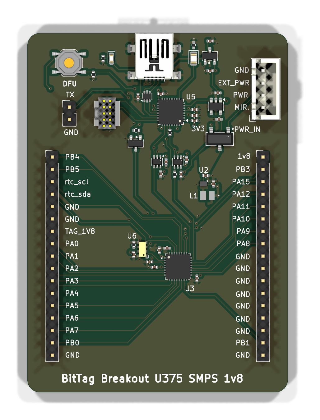
Block diagram
flowchart TB
  subgraph IF["External interface"]
    direction LR
    MCU["STM32L432<br/>ST-LINK emulation"]
    REG["XC6206 regulator"]
    USB["USB Mini-B (J104)"]
    SWD["SWD header (J102)"]
  end
  subgraph PWR["Power and measurement"]
    direction LR
    SHIFT["2 × SN74LVC1T45<br/>level shifters"]
    SWCH["SPDT slide switch<br/>supply changeover"]
    EXT["PWR_IN (J1)<br/>Joulescope"]
  end
  subgraph TAG["Tag side — what a tag would carry"]
    direction LR
    TMCU["STM32U375<br/>tag processor"]
    RTC["RV-3028-C7<br/>RTC"]
    BUCK["TPS62840 buck<br/>+ 2.2 µH"]
    REG2["AP2112K-1.8"]
  end
  subgraph CONN["Prototype interface"]
    PAIR["J3 + J4<br/>2 × 1×17 header"]
  end
  IF --- PWR
  PWR --- TAG
  TAG --- CONN
Major components
| Role | Part | Section |
|---|---|---|
| Programming processor | STM32L432KBU6 | External interface |
| Regulator | XC6206 | External interface |
| ESD | USBLC6-2P6 | External interface, on the USB port |
| Level shifters | SN74LVC1T45DCK ×2 | Between a 3.3 V interface and a 1.8 V target |
| Supply changeover | SW_SPDT | Power — LiPo line, so a physical changeover |
| Tag processor | STM32U375 | Tag side |
| Tag RTC | RV-3028-C7 | Tag side |
| Tag supply | TPS62840YBGR + 2.2 µH | Tag side — the switching converter the name refers to |
| Tag regulator | AP2112K-1.8 | Tag side |
| Prototype interface | J3, J4 — PinHeader_1x17 |
Connector pair |
What is distinctive
The SMPS in the name is a TPS62840 buck converter, with the same 2.2 µH
inductor the production IMUTag carries. That is what separates this revision
from its siblings: tag-breakout-u375-smps and tag-breakout-l432-u375-lipo-v1
supply the tag side through a TPS7A0218 LDO behind a SiP32432 load switch, where
this board replaces both with the switching converter. The prototyping hardware
followed the tag design rather than lagging it.
A 1.8 V tag side, which is why the level shifters are here. The U375 tags run their core at 1.8 V while the base's interface sits at 3.3 V, so every signal crossing between them passes through an SN74LVC1T45.
A physical supply changeover, because this is the LiPo line — the production IMUTag runs from a 12 mAh LiPo. The coin-cell breakout uses an analog switch for the same job.
It prototypes the IMUTag. Pair it with
IMUTagNandBMP581-breakout, whose BMM350,
BMP581, LSM6DSV and GD5F2GM7RE NAND are exactly the sensor and memory set of
imutag-smps.
The design review in this directory names a different board
tag-breakout-u375-smps-v1 carries
tag-breakout-l432-u375-lipo-v1-design-review.md, inherited from the board
it was copied from. Two near-identical siblings exist —
tag-breakout-u375-smps and tag-breakout-l432-u375-lipo-v1 — and this is
the one with the most recent fabrication output, including the only complete
production/ package of the three. It is also the only one of the three
carrying the switching converter, so the review — written against an
LDO-and-load-switch design — does not describe this board's power section.
Design files
Design directory on GitHub Schematic (PDF) Design review (named for a sibling board)