BitTagNG
BitTagNG is a BitTag with external memory. The schematic's own title block calls it exactly that. It keeps the BitTag idea — an accelerometer with a hardware activity state machine, a processor that sleeps between transitions — and adds a flash chip so the record is no longer bounded by the processor's internal flash.
Fabricated and tested, but possibly a dead end
This board has been built and exercised. Whether it becomes the line BitTag development continues along is not settled; it is documented here because it exists and was measured, not because it supersedes BitTagv7.
The board
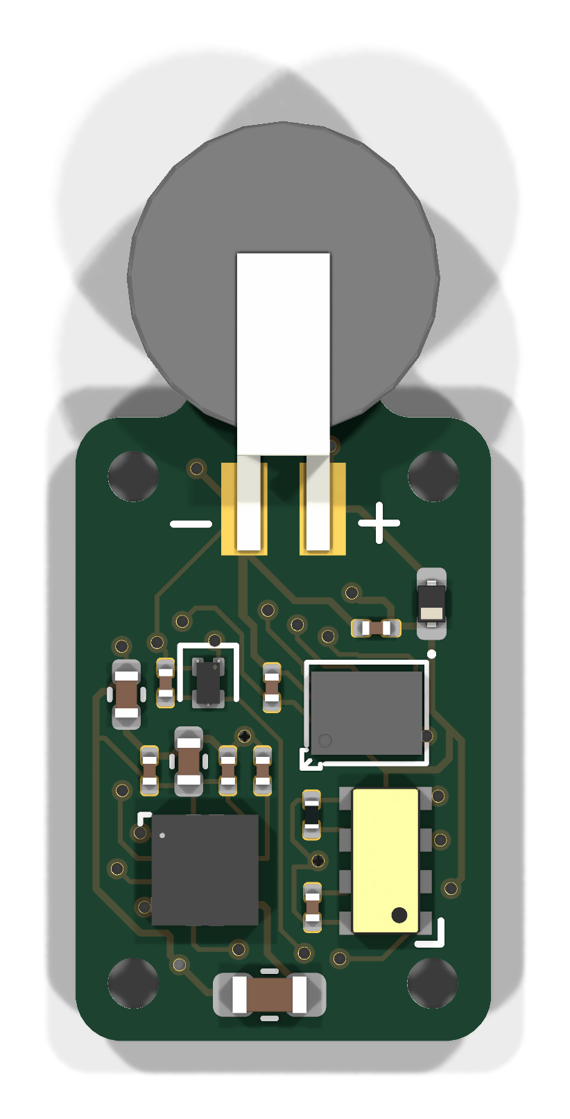
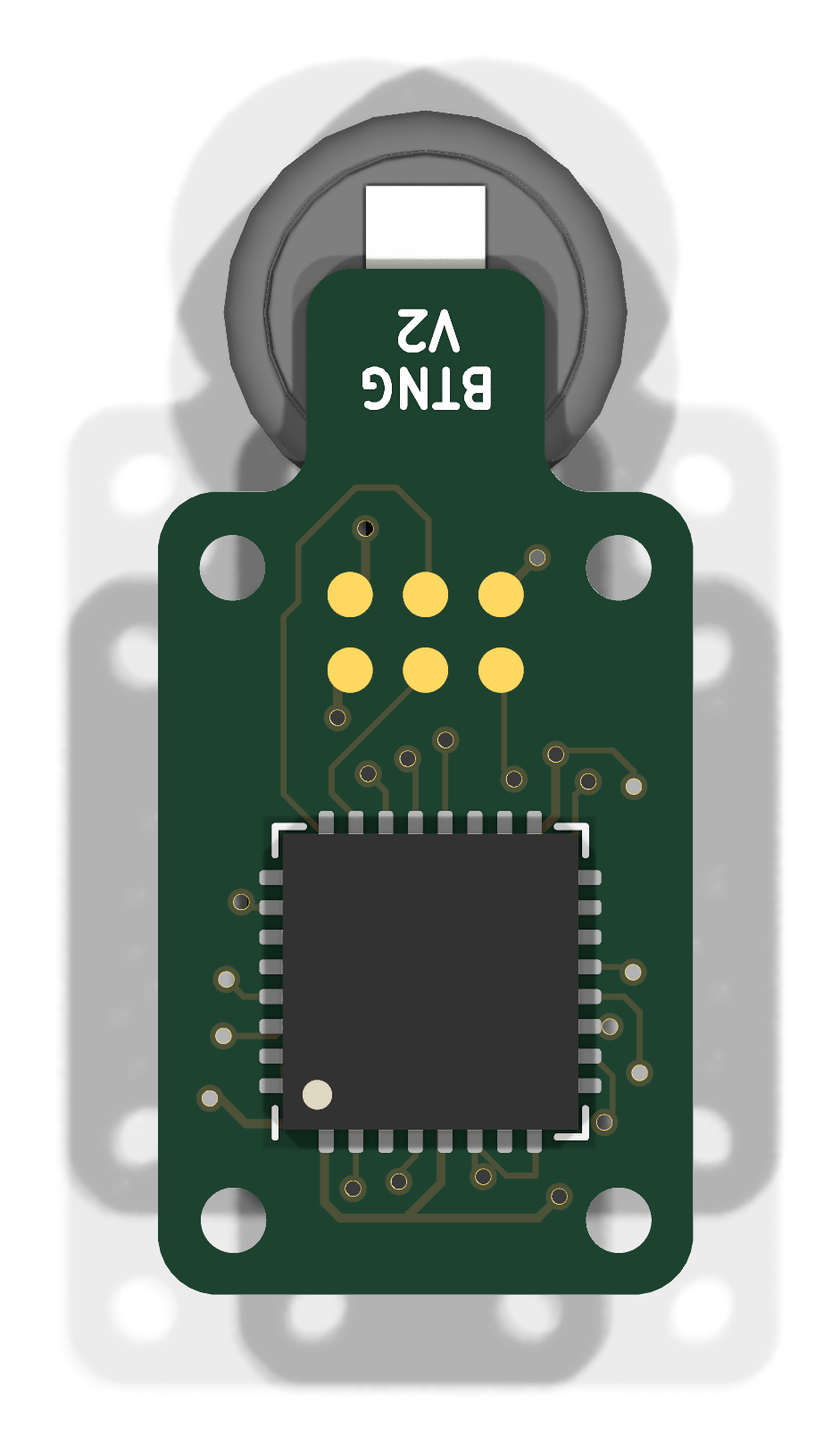
The external flash is what distinguishes this board from BitTagv7, alongside the processor, RTC and accelerometer. These are rendered from the KiCad layout by kicad-cli; see
Board Designs for how they are regenerated.
Block diagram
flowchart LR
  subgraph TAG[BitTagNG]
    direction LR
    subgraph ON[Always on]
      direction TB
      RTC["RV-3028-C7<br/>RTC"]
      MCU["STM32L432KCU6<br/>processor"]
      ACC["ADXL367<br/>accelerometer"]
      FLASH["AT25FF321A<br/>4 MB serial flash"]
      RTC --- MCU
      MCU --- ACC
      MCU --- FLASH
    end
    subgraph PWR[Power]
      BAT["MS621FE-FL11E or<br/>MS920SE-FL27E<br/>D401 Schottky"]
    end
    IF["Interface<br/>SWD + pogo pads"]
  end
  ON --- PWR
  ON --- IF
No switched section. Both the accelerometer and the flash were chosen for quiescent currents low enough to stay powered, so there is nothing a load switch would earn back.
Major components
| Role | Part | Notes |
|---|---|---|
| Processor | STM32L432KCU6 | |
| RTC | RV-3028-C7 | 32.768 kHz, 1 ppm |
| Sensor | ADXL367BCCZ | 3-axis accelerometer; successor to the ADXL362 in BitTagv7 |
| Memory | AT25FF321A-UUN | 4 MB serial flash, low quiescent current |
| Power | D401 CDBQC0130L-HF | Schottky reverse-polarity protection; no regulator |
| Battery | MS621FE-FL11E or MS920SE-FL27E | 5.5 mAh / 230 mg, or 11 mAh / 450 mg |
The power tree is one diode deep. An MS621 3 V rechargeable coin cell feeds
VBAT, D401 drops it to a VIN of roughly 2.8 V, and every device on the board
runs from that directly — processor, accelerometer, flash and RTC alike. The
binding constraint is the 3.6 V shared operating limit of the STM32 and the
ADXL367, against a 4.0 V absolute maximum on both.
The cell chemistry is not a free choice
This board takes one of two Seiko rechargeable coin cells: the MS621FE-FL11E (5.5 mAh, 230 mg) or the MS920SE-FL27E (11 mAh, 450 mg). Which one is a mass-versus-endurance decision for the deployment.
Neither may be swapped for a 3.7 V LiPo. Without a regulator the rail follows the cell, and a LiPo charged to 4.2 V would put roughly 4.0 V on it — the absolute maximum rating of both the processor and the accelerometer, not merely outside their operating range.
What it records
The same activity record as a BitTag — one bit per second, aggregated — but written to 4 MB of external flash rather than to the processor's internal flash. That is the whole point of the board: it removes the memory ceiling, so the limit on a deployment becomes the battery and the recovery date rather than the space available for records.
Power
Not measured. The five targets qualified against fw-v0.6 are
BitTag, PresTag, CompassTag, UIUCTag and IMUTag; BitTagNG is not among them.
BitTag's figures are the nearest guide — same processor, same accelerometer, same unregulated coin cell — but BitTagNG adds 4 MB of serial flash on the always-on rail, so expect its resting current to be higher.
Design files
Design directory on GitHub Schematic (PDF) Design review
The review covers the power tree and rail headroom, pinout verification across all five active devices, and the resolution of three original blocking findings.